- 您现在的位置:买卖IC网 > Sheet目录343 > MIC4103YM (Micrel Inc)IC MOSFET DRIVER 100V CMOS 8SOIC
�� �
�
�Micrel�
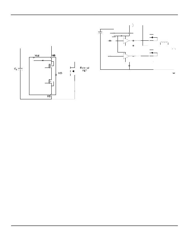
�High-Side� Driver� and� Bootstrap� Circuit�
�MIC4103/4104�
�A� block� diagram� of� the� high-side� driver� and� bootstrap�
�circuit� is� shown� in� Figure� 4.� This� driver� is� designed� to� drive�
�a� floating� N-channel� MOSFET,� whose� source� terminal� is�
�referenced� to� the� HS� pin.�
�C� VDD�
�HI�
�Vdd�
�Level�
�shift�
�HB�
�C� B�
�HO�
�Vin�
�Q1�
�Lout�
�HS�
�Q2�
�LI�
�LO�
�Vss�
�Figure� 5.� High-Side� Driver� and� Bootstrap� Circuit�
�Power� Dissipation� Considerations�
�Power� dissipation� in� the� driver� can� be� separated� into� three�
�areas:�
�?�
�Internal� diode� dissipation� in� the� bootstrap� circuit�
�Figure� 4.� High-Side� Driver� and� Bootstrap� Circuit� Block�
�Diagram�
�?�
�?�
�Internal� driver� dissipation�
�Quiescent� current� dissipation� used� to� supply� the�
�internal� logic� and� control� functions.�
�A� low-power,� high-speed,� level� shifting� circuit� isolates� the�
�low-side� (VSS� pin)� referenced� circuitry� from� the� high-side�
�(HS� pin)� referenced� driver.� Power� to� the� high-side� driver�
�and� UVLO� circuit� is� supplied� by� the� bootstrap� circuit� while�
�the� voltage� level� of� the� HS� pin� is� shifted� high.�
�The� bootstrap� circuit� consists� of� an� internal� diode� and�
�external� capacitor,� C� B� .� In� a� typical� application,� such� as� the�
�synchronous� buck� converter� shown� in� Figure� 5,� the� HS� pin�
�is� at� ground� potential� while� the� low-side� MOSFET� is� on.�
�The� internal� diode� allows� capacitor� C� B� to� charge� up� to�
�V� DD� ?� V� D� during� this� time� (where� V� D� is� the� forward� voltage�
�drop� of� the� internal� diode).� After� the� low-side� MOSFET� is�
�turned� off� and� the� HO� pin� turns� on,� the� voltage� across�
�capacitor� C� B� is� applied� to� the� gate� of� the� upper� external�
�MOSFET.� As� the� upper� MOSFET� turns� on,� voltage� on� the�
�HS� pin� rises� with� the� source� of� the� high-side� MOSFET� until�
�it� reaches� V� IN� .� As� the� HS� and� HB� pin� rise,� the� internal�
�diode� is� reverse� biased� preventing� capacitor� C� B� from�
�discharging.�
�Bootstrap� Circuit� Power� Dissipation�
�Power� dissipation� of� the� internal� bootstrap� diode� primarily�
�comes� from� the� average� charging� current� of� the� C� B�
�capacitor� times� the� forward� voltage� drop� of� the� diode.�
�Secondary� sources� of� diode� power� dissipation� are� the�
�reverse� leakage� current� and� reverse� recovery� effects� of�
�the� diode.�
�The� average� current� drawn� by� repeated� charging� of� the�
�high-side� MOSFET� is� calculated� by:�
�I� F� (� AVE� )� =� Q� gate� � f� S�
�where� :� Q� gate� =� Total� Gate� Charge� at� V� HB�
�f� S� =� gate� drive� switching� frequency�
�The� average� power� dissipated� by� the� forward� voltage� drop�
�of� the� diode� equals:�
�Pdiode� fwd� =� I� F� (� AVE� )� � V� F�
�where� :� V� F� =� Diode� forward� voltage� drop�
�November� 2010�
�11�
�M9999-110910-B�
�发布紧急采购,3分钟左右您将得到回复。
相关PDF资料
MIC4124YME
IC MOSFET DRVR DUAL NONINV 8SOIC
MIC4128YMME
IC DRIVER MOSFET 1.5A DUAL 8MSOP
MIC4129YME
IC MOSFET DRIVER 6A INVERT 8SOIC
MIC4223YM
IC MOSFET DVR DUAL-INV 4A 8-SOIC
MIC4417YM4 TR
IC DRIVER MOSF LOW SIDE SOT143-4
MIC4420ZT
IC DRIVER MOSFET 6A LS TO-220-5
MIC4422AYN
IC DRIVER MOSFET 9A LS 8-DIP
MIC4422ZT
IC DRIVER MOSFET 9A LS TO-220-5
相关代理商/技术参数
MIC4103YM TR
功能描述:功率驱动器IC 100V Half Bridge driver, 3/2A sink/Source Driver
RoHS:否 制造商:Micrel 产品:MOSFET Gate Drivers 类型:Low Cost High or Low Side MOSFET Driver 上升时间: 下降时间: 电源电压-最大:30 V 电源电压-最小:2.75 V 电源电流: 最大功率耗散: 最大工作温度:+ 85 C 安装风格:SMD/SMT 封装 / 箱体:SOIC-8 封装:Tube
MIC4104
制造商:MICREL 制造商全称:Micrel Semiconductor 功能描述:100V Half Bridge MOSFET Drivers 3/2A Sinking/Sourcing Current
MIC4104YM
功能描述:功率驱动器IC 100V HalfBridge MOSFET Driver 3/2A SOURCE/SINK CURRENT TTL INPUT (Lead Free)
RoHS:否 制造商:Micrel 产品:MOSFET Gate Drivers 类型:Low Cost High or Low Side MOSFET Driver 上升时间: 下降时间: 电源电压-最大:30 V 电源电压-最小:2.75 V 电源电流: 最大功率耗散: 最大工作温度:+ 85 C 安装风格:SMD/SMT 封装 / 箱体:SOIC-8 封装:Tube
MIC4104YM TR
功能描述:功率驱动器IC 100V HalfBridge MOSFET Driver 3/2A SOURCE/SINK CURRENT TTL INPUT (Lead Free)
RoHS:否 制造商:Micrel 产品:MOSFET Gate Drivers 类型:Low Cost High or Low Side MOSFET Driver 上升时间: 下降时间: 电源电压-最大:30 V 电源电压-最小:2.75 V 电源电流: 最大功率耗散: 最大工作温度:+ 85 C 安装风格:SMD/SMT 封装 / 箱体:SOIC-8 封装:Tube
MIC4104YML
制造商:RF Micro Devices Inc 功能描述:
MIC4120
制造商:MICREL 制造商全称:Micrel Semiconductor 功能描述:6A-Peak Low-Side MOSFET Driver
MIC4120_05
制造商:MICREL 制造商全称:Micrel Semiconductor 功能描述:6A-Peak Low-Side MOSFET Driver
MIC4120_10
制造商:MICREL 制造商全称:Micrel Semiconductor 功能描述:6A-Peak Low-Side Mosfet Driver Bipolar/CMOS/DMOS Process